Chirality and Chiroptical Effects in Plasmonic Nanostructures: Fundamentals, Recent Progress, and Outlook
V. K. Valev, J. J. Baumberg, C. Sibilia and T. Verbiest
Adv. Mater. (2013) in press.

Strong chiroptical effects recently reported result from the interaction of light with chiral plasmonic nanostructures. Such nanostructures can be used to enhance the chiroptical response of chiral molecules and could also significantly increase the enantiomeric excess of direct asymmetric synthesis and catalysis. Moreover, in optical metamaterials, chirality leads to negative refractive index and all the promising applications thereof. In this Progress Report, we highlight four different strategies which have been used to achieve giant chiroptical effects in chiral nanostructures. These strategies consecutively highlight the importance of chirality in the nanostructures (for linear and nonlinear chiroptical effects), in the experimental setup and in the light itself. Because, in the future, manipulating chirality will play an important role, we present two examples of chiral switches. Whereas in the first one, switching the chirality of incoming light causes a reversal of the handedness in the nanostructures, in the second one, switching the handedness of the nanostructures causes a reversal in the chirality of outgoing light.
Characterization of Nanostructured Plasmonic Surfaces with Second Harmonic Generation [Invited Feature Article]
V. K. Valev
Langmuir 28, 15454–15471 (2012).
Because of its high surface and interface sensitivity, the nonlinear optical technique of second harmonic generation (SHG) appears as a designated method for investigating nanostructured metal surfaces. Indeed, the latter present a high surface-to-volume ratio, but, even more importantly, they can exhibit strong near-field enhancements, or "hotspots". Hotspots often appear as a result of geometric features at the nanoscale or of surface plasmon resonances, which are collective electron oscillations at the surface that, on the nanoscale, can readily be excited by light. In the last ten years, near-field hotspots have been responsible for a dramatic development in the field of nano-optics. In this Feature Article, the influence of hotspots on the SHG response of nanostructured metal surfaces is discussed at both the microscopic and the macroscopic level. At the microscopic level, the nanostructured metal surfaces were characterized by scanning SHG microscopy, complemented by rigorous numerical simulations of the near-field and of the local electric currents at the fundamental frequency. At the macroscopic level, the SHG - Circular Dichroism and the Magnetization-induced SHG characterization techniques were employed.
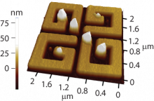
Distributing the optical near-field for efficient field-enhancements in nanostructures
V. K. Valev, B. De Clercq, C. G. Biris, X. Zheng, S. Vandendriessche, M. Hojeij, D. Denkova, Y. Jeyaram, N. C. Panoiu, Y. Ekinci, A. V. Silhanek, V. Volskiy, G. A. E. Vandenbosch, M. Ameloot, V. V. Moshchalkov, and T. Verbiest,
Adv. Mater. 24, OP208-OP215, (2012).
This work has been highlighted in ScienceDaily (July 18, 2012).

At present, the research field of plasmonics is rapidly growing and local field enhancements (hotspots) are becoming increasingly important for chemical- and bio-sensing. However, by definition, hotspots are highly localized and, for intense illumination, they can become too hot, causing damage. Here we present a nanoengineered sample pattern that, when illuminated with circularly polarized light, can distribute the optical near-field over the entire sample surface, thereby increasing the useful area and allowing the use of higher illumination intensities.
The results we show are quite counter-intuitive. Indeed, one might expect randomly oriented linearly polarized light to also distribute the optical near-field over the entire surface of the nanostructures. We show in our manuscript that this is not the case because the expectation fails to take into account the optical properties of this material: while for linearly polarized light the electron density is mainly subject to strong coupling between the nanostructures, for circularly polarized light the electron density distribution is mainly confined within them. Our findings are supported by two sets of independent theoretical simulations and by two experimental techniques – second harmonic generation scanning microscopy and plasmon-induced sub-wavelength laser-ablation.
The type of ring-shaped nanostructured samples we present can find a broad range of applications in chemical transformations, photochemical reactions, catalytic reactions and SERS; essentially, everywhere where the interaction between molecules and local field enhancements plays an important role.
Plasmon-enhanced sub-wavelength laser ablation: plasmonic nanojets
V. K. Valev, D. Denkova, X. Zheng, A. I. Kuznetsov, C. Reinhardt, B. N. Chichkov, G. Tsutsumanova, E.J. Osley, V. Petkov, B. De Clercq, A. V. Silhanek, Y. Jeyaram, V. Volskiy, P. A. Warburton, G. A. E. Vandenbosch, S. Russev, O. A. Aktsipetrov, M. Ameloot, V. V. Moshchalkov, T. Verbiest,
Adv. Mater. 24, OP29-OP35 (2012).
This work has been highlighted in Nature Photonics, ScienceDaily (January 13, 2012) and Knack.

When a pebble drops on the surface of water, it is often observed that a water column, or “back-jet”, surges upwards. Counter-intuitive though it might be, a similar phenomenon can occur when light shines on a metal film surface. Indeed, tightly focused femtosecond laser pulses carry sufficient energy to locally melt the surface of a gold film and the impact from these laser pulses produces a back-jet of molten gold with nanoscale dimensions – a nanojet.
As the name suggests, nanojets on the surface of a homogeneous gold film are quite small, their size being determined by the distribution of energy in the light pulse. This distribution of energy is in turn dependent on the wavelength of light. Consequently, although these nanojets are quite small, they cannot be much smaller than the wavelength of light. Well, we have shown that they actually can, with the help of surface plasmons.
Surface plasmons are coherent oscillations of the electron density in metal nanostructures that can readily be excited by light. Essentially, in response to the incident light’s electric field, the electron density oscillates in the plasmonic hotspots producing an electric current. Associated Ohmic losses raise the temperature of the nanomaterial within the plasmonic hotspot above the melting point. A nanojet and nonosphere ejection can then be observed precisely from the plasmonic hotspots.
U-Shaped Switches for Optical Information Processing at the Nanoscale
V. K. Valev, A. V. Silhanek, B. De Clercq, W. Gillijns, Y. Jeyaram, X. Zheng, V. Volskiy, O. A. Aktsipetrov, G. A. E. Vandenbosch, M. Ameloot, V. V. Moshchalkov, T. Verbiest,
Small 7, 2573-2576 (2011).

Fully light based circuits are becoming a realistic possibility, due to the recent advances in metamaterials. The possibility arises from the fact that light waves can couple to collective excitations of electrons at the surfaces of metallic nanostructures, a property referred to as: surface plasmon resonances.
We report on a novel way to transmit information from a beam of light to the plasmonic outputs of U-shaped nanostructures: four distinct logical states can be transmitted depending on the polarization of the incoming light. Upon coupling the output extremities of the U-shaped switches to plasmonic metamaterial waveguides, we believe that information can be channeled through an all-optical circuit.
The figure to the left representes a schematic diagram of the plasmonic switch for optical information processing at the nanometer scale. Depending on the polarization state of the incoming light (at 800 nm wavelength), the two branches (outputs A and B) of a golden U-shaped nanostructure, give rise to localized second harmonic sources (at 400 nm wavelength), or hotspots, that are due to local field enhancements. The nanostructure is 600 nm long, 400 nm wide, 25 nm thick. A and B are both 200 nm wide.
Hotspot Decorations map plasmonic patterns with the resolution of scanning probe techniques
V. K. Valev, A. V. Silhanek, Y. Jeyaram, D. Denkova, B. De Clercq, V. Petkov, X. Zheng, V. Volskiy, W. Gillijns, G. A. E. Vandenbosch, O. A. Aktsipetrov, M. Ameloot, V. V. Moshchalkov, and T. Verbiest,
Phys. Rev. Lett. 106, 226803 (2011).
This work has been highlighted in Laser Focus World, ScienceDaily (June 6, 2011), also diffused by Nanotech-Now, NanoWerk, Photonics.com, AzoOptics, AzoNano, and AlphaGalileo.
Quoting: "Imaging of Surface Plasmons May Be a Lot Easier Than Previously Thought"
An unusual observation turned into a scientific breakthrough when K.U.Leuven researchers investigating the optical properties of nanomaterials discovered that so-called surface plasmons leave imprints on the surface of the nanostructures. This led to a new type of high resolution microscopy for imaging the electric fields of nanostructures
Surface plasmon hotspots can be imprinted on metallic nanostructures for subsequent high resolution imaging with standard surface probe techniques.
Nanomaterials, consisting of extremely small particles or thin layers, tend to acquire unexpected properties. Optical nanomaterials are a class of materials that have emerged over the last ten years and that have quickly become a hot topic in material science due to their counterintuitive optical behavior and revolutionary potential applications. Optical nanomaterials are mainly based on surface plasmon resonances – the property whereby, in metallic nanostructures, light can collectively excite surface electron waves. These electron waves have the same frequency as light, but much shorter wavelengths, which allow their manipulation at the nanoscale. In other words, with the help of plasmons, light can be captured, modified and even stored in nanostructures. This emerging technology finds applications in surprising areas, ranging from cancer treatment (by targeting cancer cells with nanoparticles that will produce heat when excited) to invisibility (by causing light to follow a trail of nanoparticles, that acts as an invisibility cloak to whatever is underneath them).
The imaging of surface plasmons provides a direct way to map and understand the local electric fields that are responsible for the unusual electromagnetic properties of optical nanomaterials. However, the imaging of surface plasmons is quite challenging. While there are methods to image plasmons with high resolution, they come at a considerable increase in both cost and complexity. But now, Ventsislav K. Valev and his colleagues have demonstrated a powerful and user friendly method for imaging plasmonic patterns in nanostructures.
"We were performing routine characterization of freshly grown samples, when I asked Yogesh, one of our Ph.D. students, to look at a sample that had already been studied. There was absolutely no reason to do this; I just had a hunch," sais Ventsislav Valev. "Surprisingly, this sample appeared to be decorated and I immediately recognized the pattern. Somehow, the optical properties have been imprinted on the surface of the nanostructures."
The scientists indeed found out that upon illuminating nanostructures made of nickel or palladium, the resulting surface plasmon pattern is imprinted on the structures themselves. This imprinting is done through displacing material from the nanostructure to the regions where the plasmon enhancements are the largest. In this manner, the plasmons are effectively decorated, allowing for subsequent imaging with standard surface probe techniques, such as scanning electron microscopy or atomic force microscopy. The imprinting method is quite unique, combining aspects of both imaging and writing techniques."
Plasmons reveal the direction of magnetization in nickel nanostructures
V. K. Valev, A. V. Silhanek, W. Gillijns, Y. Jeyaram, H. Paddubrouskaya, A. Volodin, C. G. Biris, N. C. Panoiu, B. De Clercq, M. Ameloot, O. A. Aktsipetrov, V. V. Moshchalkov, T. Verbiest,
ACS Nano, 5, 91-96 (2011).
The development of nanophotonics, nanoelectronics and nanomagnetics could result in new generations of devices, capable to store and process information at increasing speed and decreasing energy cost. However, the relationship between these three nanotechnologies is only beginning to be clarified. The influence of magnetic fields on surface plasmons combines aspects of photonics, electronics and magnetics at the nano scale. Surface plasmons are collective excitations of electrons under the influence of light’s electromagnetic field and, in magnetic materials, these electrons can experience the effects of externally applied magnetic fields as well.
We have applied the surface-sensitive nonlinear optical technique of magnetization-induced second harmonic generation (MSHG) to plasmonic, magnetic nanostructures made of Ni. We show that surface plasmon contributions to the MSHG signal can reveal the direction of the magnetization. Both the plasmonic and the magnetic nonlinear optical responses can be tuned; our results indicate novel ways to combine nanophotonics, nanoelectronics, and nanomagnetics and suggest the possibility for large magneto-chiral effects in metamaterials.
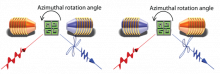
Figure 1. Magnetization-induced second harmonic generation is measured in four-fold symmetric magnetic, plasmonic nanostructures. Upon rotating the sample in the presence of this magnetic field, the second harmonic generation intensity yields a four-fold pattern that is asymmetric, i.e. it resembles a ratchet wheel. Interestingly, upon reversing the direction of the externally applied magnetic field, the direction of the ratchet wheel reverses as well.
Linearly polarized second harmonic generation microscopy reveals chirality
V. K. Valev, A. V. Silhanek, N. Smisdom, B. De Clercq, W. Gillijns, O. A. Aktsipetrov, M. Ameloot, V. V. Moshchalkov, T. Verbiest,
Optics Express, 18, 8286-8293 (2010) & Optics Express, 19, 9242-9244 (2011).
In optics, chirality is typically associated with circularly polarized light. Here we present a novel way to detect the handedness of chiral materials with linearly polarized light. We performed Second Harmonic Generation (SHG) microscopy on G-shaped planar chiral nanostructures made of gold. The SHG response originates in distinctive hotspots, whose arrangement is dependent of the handedness, see Figure 1. These results uncover new directions for studying chirality in artificial materials.
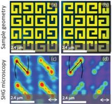
Figure 1. Schematic diagram of the sample geometry of the G-shaped and of the mirror-G shaped sample structures, in a) and b) respectively. In c) and d), the SHG microscopy images of the G-shaped and of the mirror-G shaped sample structures respectively. The white arrows indicate the direction of the linear polarization. The color coded intensities increase from purple, through green, then yellow to red.
Asymmetric second harmonic generation from chiral G-shaped gold nanostructures
V. K. Valev, A. V. Silhanek, N. Verellen, W. Gillijns, P. Van Dorpe, G.A.E. Vandenbosch, O. A. Aktsipetrov, V. V. Moshchalkov, T. Verbiest,
Phys. Rev. Lett. 104, 127401 (2010).
We reported on a new optical phenomenon, in which the chirality of a patterned thin film is revealed by sample rotation - a unique and counterintuitive procedure, since chirality is normally invariant under rotation symmetry. This effect is illustrated in Figure 1, where upon azimuthal sample rotation, the SHG pattern is represented as a ratchet wheel that changes its direction of rotation with the handedness configuration [G and mirror-G]. This novel property involves solely linearly polarized light.
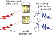
Figure 1. A schematic diagram of the Assymmetric Second Harmonic Generation (ASHG) effect. The effect consists in distinguishing the handedness of a chiral material by rotating the sample in an experiment involving solely linearly polarized light.
It should also be noted that until now, all known optical effects sensitive to chirality contained an electric dipole contribution. Because a distinction in the peak intensity is also observed in an electric dipole forbidden configuration, ASHG is the first effect to occur without an electric dipole contribution.
Plasmonic ratchet wheels: switching circular dichroism by arranging chiral nanostructures
V. K. Valev, N. Smisdom, A. V. Silhanek, B. De Clercq, W. Gillijns, M. Ameloot, V. V. Moshchalkov and T. Verbiest,
Nano Lett. 9, 3945 (2009).
We demonstrated circular dichroism (CD) in the second harmonic generation (SHG) signal from chiral assemblies of G-shaped nanostructures made of gold. The arrangement of the G shapes was crucial since upon reordering them the SHG-CD effect disappeared. In Figure 1, a schematic diagram of this phenomenon can be seen.
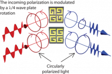
Figure 1. A schematic diagram of the switching of circular dichroism by arranging chiral nanostructures.
Microscopy revealed SHG “hotspots” assemblies, which originate in enantiomerically sensitive plasmon modes, having the novel property of exhibiting a chiral, ratchet-wheel-type geometry themselves in relation with the handedness of the material. These results open new frontiers in studying chirality.
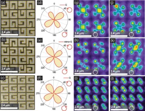
Figure 2. In (a), (b) and (c), Scanning Electron Microscopy pictures of the samples with G- and mirror-G-shape structures. The yellow lines have been added around the edges of the structures in order to improve the visibility. In (d), (e) and (f), the SHG intensity as function of the angle of rotation of a quarter wave plate. The oriented circles indicate the directions for left- and right-hand circularly polarized light. The polarizer-analyzer combination was P-S. SHG microscopy images with right-hand circularly polarized light in (g), (h) and (i) and with left-hand side circularly polarized light in (j), (k) and (l). The colour coded intensities increase from purple, through green, then yellow, to red.
In Fig 2a and 2b, the arrangement of the sample structures is presented. Both figures are mirror images of each other. Next to them, the red curves reveal a CD effect, i.e. there is more SHG generated for one circularly polarized light than for the other. This can be seen in the fact that the larger yellow lobes are directed towards the right-hand oriented circle in Fig. 2d, while they are along the left-hand oriented circle in Fig. 2e. However, when the sample structures are arranged differently, see Fig. 2c, the SHG-CD effect disappears, see the corresponding red curve in Fig. 2f, where no yellow lobe is larger than another.
The source of this astonishing property became apparent with SHG-microscopy. It was shown that the SHG signal originates in SHG hotspots and it was found out that for differently oriented circularly polarized light (see Fig. 2g and 2j) different plasmon modes are excited in the structures. This was confirmed upon imaging the opposite sample handedness (see Fig. 2h and 2k). Clearly, the arrangement of the nanostructures plays a crucial role since upon reordering them the SHG-CD effect vanishes (see Fig. 2i and 2l).
In particular, in Fig 2g, the SHG sources form a rather homogeneous central square that connects all four Gs in the structure's unit cell, see Fig. 2a. Surrounding the square, are four "hotspots", which exhibit a comet-like shape that leads to an overall ratchet wheel pattern. Depending on the handedness of the nanostructures, this ratchet wheel pattern exhibits a different sense of rotation (see Fig. 2g and 2k). This dependence allows for the unprecedented possibility to optically determine the handedness of a material by observing it with a single circularly polarized light, i.e. no comparison with another handedness or another direction of the circularly polarized light is necessary.
